Products
|
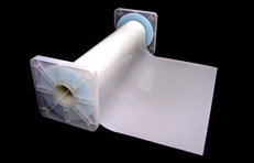
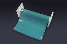
Information of Substrate Materials for Semiconductor Packages Factory
|
Features
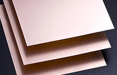
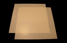
Higher reliability, better warpage control and thinner thickness. Material performance required for recent substrates and PCBs can be achieved by LαZ® which has excellent material property such as low CTE, high TG and high modulus.
Applications
Electronic Circuit
Package substrate, etc.
For applications that require higher reliability, better warpage control and thinner thickness boards for package substrates.
Specifications
| Unit | LαZ | |
|---|---|---|
| BLα-3700GS | ||
| Tg(by DMA) | ℃ | 200 |
| Tg(by TMA) | ℃ | 180 |
| CTE1 | ppm/℃ | 35 |
| CTE2 | ppm/℃ | 120 |
| Tensile Modulus(R.T.) | G Pa | 5 |
| Tensile Modulus(250℃) | G Pa | 0.2 |
| Dielectric constant | (1GHz) | 3.1 |
| Dielectric Dissipation Factor | (1GHz) | 0.012 |
| Moisture Absorption | wt% | 1.0 |
| (0.2t)(PCT-2hr/121℃) |
- 2026/06/25ProductsExpansion of Production Capacity for Semiconductor Encapsulation Materials at Sumitomo Bakelite (Suzhou) Co., Ltd.
- 2026/06/01ProductsDevelopment of High-Tg Epoxy Molding Compounds for Next-Generation SiC Power Modules
- 2026/05/18ProductsAnnouncement of Trial Launch of Liquid Encapsulant for Advanced Packages
- 2026/05/15ProductsParticipation in “ECTC 2026”
- 2026/05/14ProductsPrice Revision of Epoxy Resin Molding Compounds for Encapsulation of Semiconductor Devices SUMIKON™ EMEs
Call or email us about our Division/Department.
 Inquiry
- TEL:
- +81-3-5462-4015
- FAX:
- +81-3-5462-4883
※9:00-17:40 Mon.-Fri. (JST)