We embody the dreams of our customers and work together with them from developing to
evaluating.
Sumitomo Bakelite's technology is reflected not only in our materials, but also in our
customers' applications and processes.
・Back-end development support for advanced
semiconductors
・Support for mobility and new applications (electronic components, industry, etc.)

IT Materials Division
Become a materials solutions provider
that gives dreams
for the future of
electronics and mobility.
Latest information
- 2026/10/09ProductsExpansion of Production Capacity for Advanced Semiconductor Encapsulation Materials in Suzhou, China, and Singapore
- 2026/08/18ProductsDevelopment of a Next-Generation 3D Power Module with Ultra-Compact Size and High Power Density
- 2026/08/07ExhibitionSEMICON TAIWAN 2026 [2026/9/2-4]
- 2026/06/25ProductsExpansion of Production Capacity for Semiconductor Encapsulation Materials at Sumitomo Bakelite (Suzhou) Co., Ltd.
- 2026/06/01ProductsDevelopment of High-Tg Epoxy Molding Compounds for Next-Generation SiC Power Modules
The strengths of Sumitomo Bakelite
Point01
Lineup for all packages
in semiconductor package
manufacturing
As a provider of materials solutions,
we
offer a wide range of support to the supply chain
from the upstream to the downstream of the
semiconductor manufacturing.
Semiconductor
manufacturing processes
-
Pre-process
-
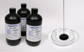
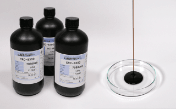
Photosensitive materials for semiconductor wafer protection. Features such as high insulation and excellent chemical resistance contribute to improved reliability in semiconductor devices. SUMIRESIN COAT “CRC” are mainly positive photosensitive materials that do not require solvents and are environmentally friendly.
-
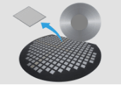
Dicing
-
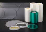
A film that prevents chips from scattering during the dicing process. It has excellent antistatic properties and is widely used in the dicing process for wafers with fine patterns.
-
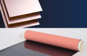
Package Substrate Creation
-
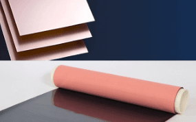
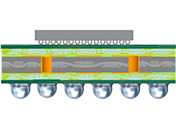
Low expansion, low dimensional change and high stiffness packaging substrate material that contributes to smaller and thinner packages. Contributes to the miniaturization of components in smartphones.
-
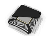
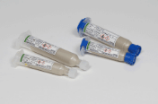
Die bonding
-
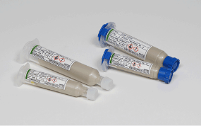
Die bonding paste for a variety of packages. Used for bonding chips and ensuring thermal diffusion.
-
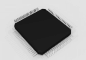
Encapsulation
-
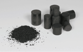
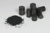
Epoxy encapsulants for semiconductors that can be used in a variety of applications and package forms. We also respond to the evolution of molding processes as semiconductors evolve.
-
Delivery
-
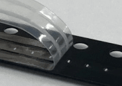
This tape is used to transport semiconductor packages and electronic components to the surface mount process. Our products have excellent antistatic properties.

Point02
Global expansion
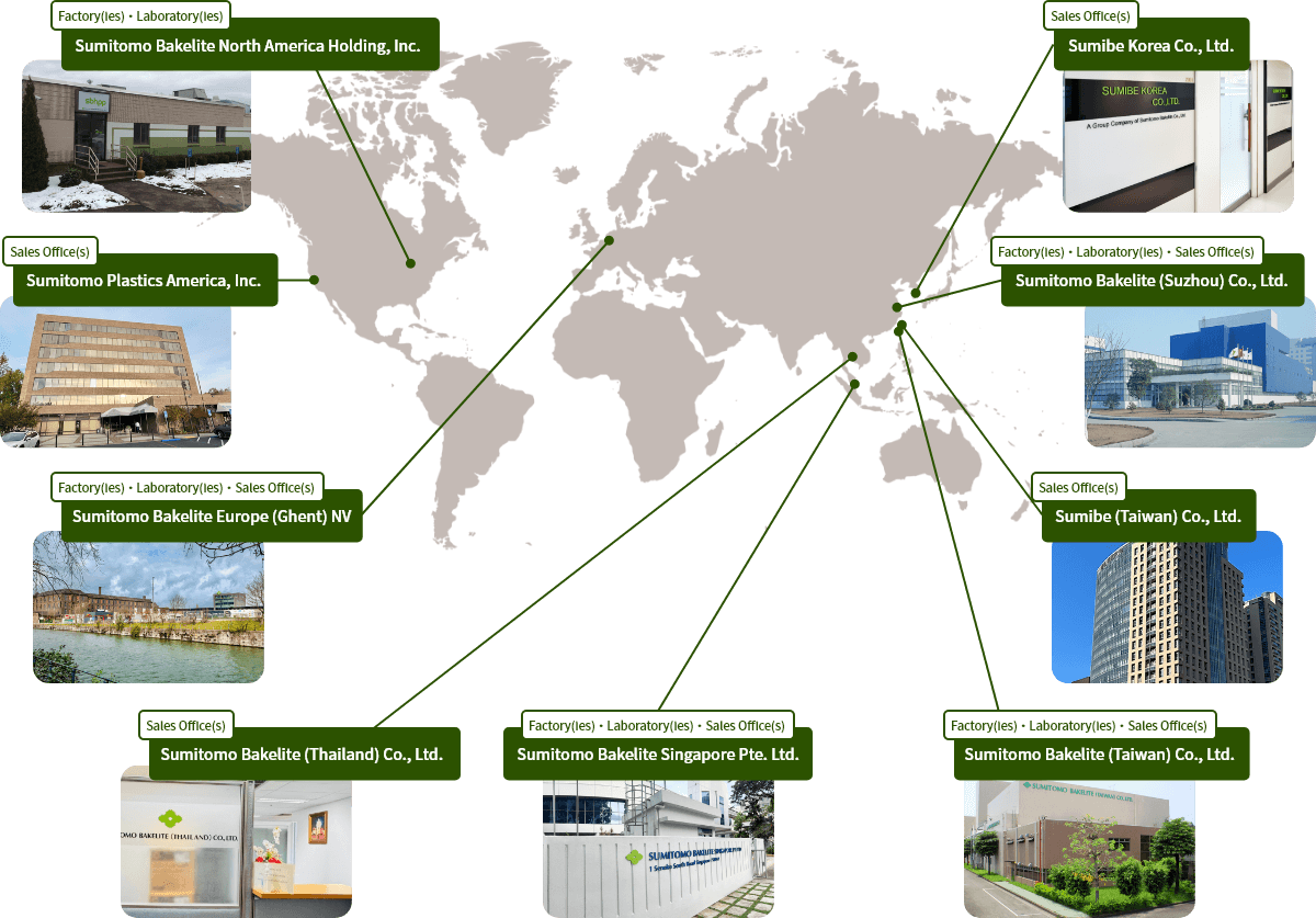
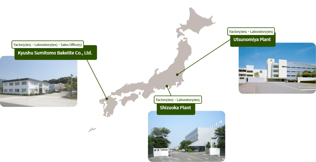
We have factories and laboratories in major markets around
the world,
enabling us to develop original products
that meet the needs of
each region and respond quickly to customer requests.
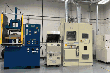
Open Lab (Open Labs)
The Sumitomo Bakelite Group supports the "imagination" and
"creativity" of its customers
and operates open laboratories (customer laboratories) in
Japan, Asia, Europe and the United States
where actual molding operations and structural and
process studies can be conducted.
Point03
R&D capabilities to respond
to the evolution of semiconductor
packaging
Collaborate with equipment manufacturers, raw material
component manufacturers,
universities, and consortia to accelerate development.
We will
provide products that respond to market information and customer needs.

Use Cases

Sumitomo Bakelite's
Solution
We are introducing Sumitomo Bakelite's diverse solutions on our special website.
New solutions are being created not only from Sumitomo Bakelite's problem-solving
proposals,
but also from proposals for customer utilization methods.