Products
|
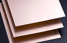
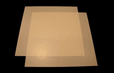
Information of Substrate Materials for Semiconductor Packages Factory
|
Features
Higher reliability, better warpage control and thinner thickness. Material performance required for recent substrates and PCBs can be achieved by LαZ® which has excellent material property such as low CTE, high TG and high modulus.
Applications
Electronic Circuit
Package substrate, etc.
For applications that require higher reliability, better warpage control and thinner thickness boards for package substrates.
Specifications
| Item | Unit | Grade | |||||||
|---|---|---|---|---|---|---|---|---|---|
| LAZ-4785TH-M | LAZ-4785TH-JB | LAZ-4785GH-J | LAZ-4785TH-G | LAZ-4785GH-G | ELC-4785TH-B | LAZ-4785GS-BA | |||
| Glass Cloth Type | - | Low CTE | Low CTE | Normal | Low CTE | Normal | Low CTE | Normal | |
| CTE1 xy | ppm/°C | 1.6 | 2 | 5 | 4 | 7 | 6 | 10 | |
| CTE1 z | ppm/°C | 12 | 12 | 12 | 12 | 12 | 12 | 16 | |
| Tg [by DMA] | ppm/°C | 210 | 280 | 280 | 255 | 255 | 265 | 265 | |
| Tensile Modulus |
@30°C | GPa | 35 | 34 | 32 | 32 | 31 | 32 | 29 |
| @250°C | GPa | 18 | 26 | 21 | 21 | 20 | 21 | 18 | |
| Dielectric Constant (1GHz) | - | 4.1 | 4.3 | 4.3 | 4.0 | 4.2 | 4.0 | 4.2 | |
| Dissipation Factor (1GHz) | - | 0.008 | 0.007 | 0.007 | 0.005 | 0.005 | 0.006 | 0.007 | |
| Peel Strength (Cu12um VLP) | kN/m | 0.9 | 0.7 | 0.7 | 0.7 | 0.7 | 0.7 | 0.8 | |
| Water Absorption (PCT-2hrs/121°C) |
wt% | 0.4 | 0.4 | 0.4 | 0.4 | 0.4 | 0.4 | 0.4 | |
Topics More
- 2024/03/13 Products Completion ceremony of the new plant for Encapsulation of Semiconductor Devices at Sumitomo Bakelite (Taiwan) Co., Ltd.
- 2022/09/29 Products Sumitomo Bakelite (Suzhou) Co., Ltd. builds a new plant for Encapsulation of Semiconductor Devices
- 2022/04/14 Products New lineup of Photosensitive Materials for Mini/Micro LED displays
- 2021/10/18 Products Launch of IoT Solution Gallery
Exhibitions More
- 2021/01/11CES 2021
- 2021/01/20CAR-ELE JAPAN 2021
Substrate Materials for Semiconductor Packages
Call or email us about our Division/Department.
 Inquiry
- TEL:
- +81-3-5462-4015
- FAX:
- +81-3-5462-4883
※9:00-17:40 Mon.-Fri. (JST)